- 您现在的位置:买卖IC网 > Sheet目录315 > BD6081GVW-E2 (Rohm Semiconductor)IC LED DRIVER BACKLIGHT 63SBGA
�� �
�
�BD6081GU,BD6081GVW�
�Technical� Note�
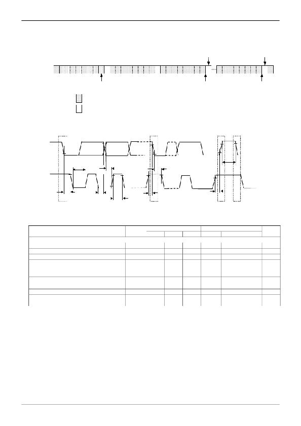
�?� Writing� protocol�
�A� register� address� is� transferred� by� the� next� 1� byte� that� transferred� the� slave� address� and� the� write-in� command.� The� 3rd�
�byte� writes� data� in� the� internal� register� written� in� by� the� 2nd� byte,� and� after� 4th� byte� or,� the� increment� of� register� address� is�
�carried� out� automatically.� However,� when� a� register� address� turns� into� the� last� address� (1Ah),� it� is� set� to� 00h� by� the� next�
�transmission.� After� the� transmission� end,� the� increment� of� the� address� is� carried� out.�
�S� X� X� X� X� X� X� X� 0� A� A7� A6� A5� A4� A3� A2� A1� A0� A� D7� D6� D5� D4� D3� D2� D1� D0� A�
�*1�
�*1�
�D7� D6� D5� D4� D3� D2� D1� D0� A� P�
�slave� address�
�R/W=0(write)�
�register� address�
�DATA�
�register� address�
�increment�
�DATA�
�register� address�
�_�
�from� master� to� slave�
�from� slave� to� master�
�A=acknowledge(SDA� LOW)�
�A=not� acknowledge(SDA� HIGH)�
�S=START� condition�
�P=STOP� condition�
�*1:� Write� Timing�
�●� Timing� diagram�
�SDA�
�t� BUF�
�SCL�
�t� LOW�
�t� SU;DAT�
�t� HD;STA�
�t� HD;STA�
�t� HD;DAT�
�t� SU;STA�
�t� SU;STO�
�S�
�t� HIGH�
�Sr�
�P�
�S�
�●� Electrical� Characteristics(Unless� otherwise� specified,� Ta=25� ℃� ,� VBAT=3.6V,� VIO=1.8V)�
�Parameter� Symbol�
�Standard-mode�
�Min.� Typ.� Max.� Min.�
�Fast-mode�
�Typ.� Max.�
�Unit�
�【� I� 2� C� BUS� format� 】�
�SCL� clock� frequency�
�LOW� period� of� the� SCL� clock�
�HIGH� period� of� the� SCL� clock�
�Hold� time� (repeated)� START� condition�
�After� this� period,� the� first� clock� is� generated�
�f� SCL�
�t� LOW�
�t� HIGH�
�t� HD;STA�
�0� -� 100� 0�
�4.7� -� -� 1.3�
�4.0� -� -� 0.6�
�4.0� -� -� 0.6�
�-�
�-�
�-�
�-�
�400�
�-�
�-�
�-�
�kHz�
�μ� s�
�μ� s�
�μ� s�
�Set-up� time� for� a� repeated� START� condition� t� SU;STA�
�4.7� -� -� 0.6�
�-�
�-�
�μ� s�
�Data� hold� time�
�Data� set-up� time�
�Set-up� time� for� STOP� condition�
�Bus� free� time� between� a� STOP�
�and� START� condition�
�t� HD;DAT�
�t� SU;DAT�
�t� SU;STO�
�t� BUF�
�0� -� 3.45� 0�
�250� -� -� 100�
�4.0� -� -� 0.6�
�4.7� -� -� 1.3�
�-�
�-�
�-�
�-�
�0.9�
�-�
�-�
�-�
�μ� s�
�ns�
�μ� s�
�μ� s�
�www.rohm.com�
�?� 2011� ROHM� Co.,� Ltd.� All� rights� reserved.�
�11/35�
�2011.04� -� Rev.A�
�发布紧急采购,3分钟左右您将得到回复。
相关PDF资料
BD6083GUL-E2
IC LED DRIVER BKLT 36VCSP50L3
BD6085GUL-E2
IC LED DRIVER BKLT 35VCSP50L3
BD6088GUL-E2
IC LED DRIVER BKLT 36VCSP50L3
BD6142AMUV-E2
IC LED DRIVER SGL STEP UP 24QFN
BD6581GU-E2
IC LED DVR WHT BCKLGHT VCSP85H2
BD6583MUV-AE2
IC LED DRIVER WHIT BCKLGT 24VQFN
BD6586MUV-E2
IC LED DRVR WHITE BCKLGT 24-VQFN
BD6592MUV-E2
IC LED DRVR WHITE BCKLGT 24-VQFN
相关代理商/技术参数
BD6082GUL-E2
制造商:ROHM Semiconductor 功能描述:IC BD6082GUL-E2
BD6083GUL
制造商:ROHM 制造商全称:Rohm 功能描述:Multifunction Backlight LED Driver for Small LCD Panels (Charge Pump Type)
BD6083GUL_10
制造商:ROHM 制造商全称:Rohm 功能描述:Multifunction Backlight LED Driver for Small LCD Panels (Charge Pump Type)
BD6083GUL-E2
功能描述:IC LED DRIVER BKLT 36VCSP50L3 RoHS:是 类别:集成电路 (IC) >> PMIC - LED 驱动器 系列:- 标准包装:6,000 系列:- 恒定电流:- 恒定电压:- 拓扑:开路漏极,PWM 输出数:4 内部驱动器:是 类型 - 主要:LED 闪烁器 类型 - 次要:- 频率:400kHz 电源电压:2.3 V ~ 5.5 V 输出电压:- 安装类型:表面贴装 封装/外壳:8-VFDFN 裸露焊盘 供应商设备封装:8-HVSON 包装:带卷 (TR) 工作温度:-40°C ~ 85°C 其它名称:935286881118PCA9553TK/02-TPCA9553TK/02-T-ND
BD6084GUL
制造商:ROHM 制造商全称:Rohm 功能描述:8 LEDs ALC* and LDO 4ch
BD6085GUL
制造商:ROHM 制造商全称:Rohm 功能描述:Silicon Monolithic Integrated Circuit
BD6085GUL_11
制造商:ROHM 制造商全称:Rohm 功能描述:Multifunction Backlight LED Drivers for Small LCD Panels (Charge Pump Type)
BD6085GUL-E2
功能描述:IC LED DRIVER BKLT 35VCSP50L3 RoHS:是 类别:集成电路 (IC) >> PMIC - LED 驱动器 系列:- 标准包装:6,000 系列:- 恒定电流:- 恒定电压:- 拓扑:开路漏极,PWM 输出数:4 内部驱动器:是 类型 - 主要:LED 闪烁器 类型 - 次要:- 频率:400kHz 电源电压:2.3 V ~ 5.5 V 输出电压:- 安装类型:表面贴装 封装/外壳:8-VFDFN 裸露焊盘 供应商设备封装:8-HVSON 包装:带卷 (TR) 工作温度:-40°C ~ 85°C 其它名称:935286881118PCA9553TK/02-TPCA9553TK/02-T-ND